Applied Materials VLSI panel says AI chip profits move to packaging
Applied Materials published a VLSI panel recap where executives from Nvidia, Intel, and Samsung focus on advanced packaging—chiplets and 3D stacking—as the…
Edward Mullen ·
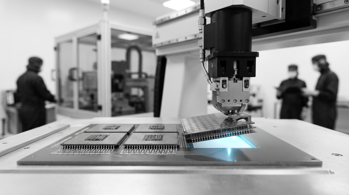
Conventional wisdom dictates that silicon's steady march towards smaller transistors dictates the pace and profitability of AI. Yet, a recent gathering of industry titans quietly upended this long-held belief. The next battleground for AI compute, they suggest, lies not solely in the wafer fab, but in the sophisticated and costly realm of multi-chiplet integration and advanced packaging.
Three giants, one message: scaling limits are now a stack problem Applied Materials’ recap of its VLSI panel places Nvidia, Intel, and Samsung in rare public alignment: performance is colliding with limits not only in transistors, but in how dies are connected and assembled. The write-up frames the challenge across design, process, and system integration—an important reframing for executives who have treated process-node shrinks as the default performance roadmap. Coming from a process and equipment vendor with visibility across fabs and assembly, the emphasis on integration is itself a data point: attention at the top of the stack is drifting toward where dies meet.
Because the Applied Materials write-up does not provide
Packaging as the next lever—chiplets and vertical integration by assembly The missing numbers: cost, yield, and where margins migrate Why “just shrink the node” is the wrong 2026 playbook A procurement and org-chart story hiding in a technical panel The skeptic’s case: process wins and memory constraints keep margins on die There is an obvious counterargument that process scaling and memory supply, not packaging, will set the cadence of AI performance, leaving margins anchored in cutting-edge wafer processes. Skeptics can also point out that chiplet schemes introduce new failure planes, that assembly yields can erase theoretical performance gains, and that supply of high-density memory and substrates can act as the dominant limiter. Because the Applied Materials write-up does not provide comparative data or independent validation, these counters remain live—and any buyer should treat the panel as hypothesis, not settled fact.
What changes for 2026 roadmaps if packaging leads
How to read the next six months of signals What the panel didn’t say out loud: the margin math plied Materials’ post, the panel highlights advanced packaging—chiplets and 3D stacking—as the next frontier for performance gains. Read plainly, that shifts the locus of compute improvement from smaller transistors on a single die to stitching multiple specialized dies together with dense, short-reach interconnects in the same package. For executives planning AI infrastructure, the relevant change is not just technical; it’s economic. If real-world throughput now depends as much on interposer density, bump pitch, thermals, and assembly yield as it does on transistor density, then the profit pools start to migrate from wafer-only metrics to multi-die integration competence. The Applied Materials blog does not publish cost, yield, or throughput figures; it offers a directional claim that “challenges span the entire technology stack” and presents packaging as a critical path. Without explicit deltas versus monolithic baselines or disclosure of failure modes, it is marketing-tier evidence. But even that absence is informative for procurement: when vendors talk packaging but withhold per-die yield or assembly fallout, assume that variability and learning-curve effects are now first-order drivers of delivered performance-per-dollar. That moves commercial leverage toward the small set of players who can repeatedly integrate multiple dies and memory in volume, and away from a worldview where transistor counts alone decide margins. Applied Materials’ panel summary pushes against that framing A popular read is that the way out of AI’s compute squeeze is better lithography, more transistor density, and faster single-die GPUs. Applied Materials’ panel summary pushes against that framing by elevating integration complexity as the limiter and packaging as the gain.
If that’s correct, then monolithic-only roadmaps underweight two hard realities: the thermal and signaling tax of long on-board traces versus in-package links, and the compounding yield penalty of very large dies. Chiplets and stacking reassign that optimization, letting designers bin smaller dies and specialize functions—if, and only if, the assembly technology and supply chain can keep pace.
For buyers of AI systems, this reframing means supplier qualification must move upstream into assembly and packaging capability, not just process node, TDP, and memory bandwidth line items. Expect due diligence to probe packaging flows, assembly partners, and integration yields alongside die specs.
Internally, chip designers will tilt more headcount and budget toward physical integration, thermal co-design, and package-aware architecture, while foundry-adjacent organizations that master multi-die assembly become price setters rather than price takers. For manufacturing leaders, that implies different bottlenecks on the line—more metrology and reliability screening around interposers and stacked vias, and different failure signatures than wafer-only defects.
If packaging is the next lever, expect foundries and integrators to pull for larger pre-commits around assembly capacity, and for chip designers to gate product launches on package reliability sign-off as much as on tape-out. Contract language will start naming integration yields and thermal budgets as shared obligations, not one-sided vendor promises.
On the factory floor, advanced assembly and inspection steps become schedule-critical, with staffing and tooling plans reflecting the fact that small variances in package flatness, warpage, or via integrity now show up directly as system-level performance variance. In software, hardware-aware compilers and schedulers will increasingly target package topology, not just die-level cores.
Because this is a vendor blog and not a peer-reviewed study, the burden of proof shifts to the market. Watch whether major chip designers publicly emphasize multi-die integration in product teases and technical overviews, and whether foundries and assembly providers foreground packaging capacity in investor communications.
Pay attention to design-tool releases and reference flows that explicitly encode package-aware partitioning and thermal co-design, a tell that teams are reorganizing around integration. Finally, track procurement language and RFPs from large buyers: if packaging process terms and integration KPIs start appearing beside process-node specs, the margin migration is underway.
Any of these would corroborate the panel’s framing; their absence would keep the monolithic-first playbook intact.
Applied Materials’ post frames the technical pivot but omits the economics: who captures the dollars when performance depends on assembly? If multi-die integration drives delivered throughput, then pricing power accrues to the scarce capability—advanced packaging lines with proven yields at scale.
That would recast negotiations between design houses and manufacturing partners, making guaranteed integration performance a billable premium rather than a bundled afterthought. The omission matters because it is where procurement decisions, not benchmarks, will decide who wins the next wave of AI hardware revenue.